PCB Manufacture Meet Industry Standards
PCBs are the backbone of modern electronics, connecting tiny electronic components with a larger circuit board. They also carry signals to and from those components, a process known as signal flow. In order to be able to do all of this, PCBs must be made from a variety of materials, with precise connections between layers. This is all made possible by a process called soldering, and the quality of that soldering is essential to the reliability of your PCB. Luckily, there are strict standards and certifications that every pcb manufactures must meet in order to produce the best possible products.
The Institute of Printed Circuits, or IPC, is a globally recognized organization that develops and publishes industry standards. These standards govern everything from design guidelines and manufacturing processes to assembly, inspection, and testing. Following these guidelines ensures that a pcb manufactures produces high-quality products, meets industry standards, and keeps up with technological advancements.
In order for a pcb to be fabricated, the original design files must be sent to the manufacturer in the correct format. This helps avoid any errors or lost information that may occur if the files are not transferred properly. Once the files have been correctly transmitted, the fabrication process begins.
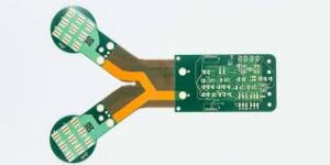
How Does a PCB Manufacture Meet Industry Standards?
First, the substrate material is applied, and then the copper layer is pre-bonded to it. The copper is what carries electrical signals throughout the board, and it can either be a thin sheet of foil or a full-on copper coating. This layer is then etched away to reveal the blueprint beneath it.
After the etching is complete, a technician uses a special machine to align the layers of the PCB. The holes from earlier are used to align the inner and outer layers of the PCB, and once the alignment is perfect, a machine known as an automatic optical inspection machine — or AOI machine for short — can perform a thorough visual inspection of the PCB. The AOI machine looks for any defects such as poor soldering or unaligned layers, and it does so by using a series of high-powered cameras positioned at different angles to view the PCB.
Once the AOI machine has found no defects, the PCB is then ready for assembly. The components are then carefully placed on the PCB, and the traces that connect them are soldered together with precision. This is followed by a final inspection and rigorous tests to make sure the PCB works as it should.
While the manufacturing process of a pcb is complex, it’s important for a manufacturer to keep up with the latest technology in order to stay competitive. Following industry standards like the IPC helps reduce the time and cost of production, improves product quality, and ensures that the resulting product will be reliable in its intended use. Adhering to these standards helps ensure that the finished product will meet and exceed customer expectations and regulatory requirements. In addition, adhering to these standards allows manufacturers to streamline the development and manufacturing processes, ensuring that they have the resources necessary to adapt to future technological advancements.