Micro Vias Help
As components continue to shrink, designers need to find ways to increase the density of their PCBs. This is where micro vias come into play, allowing engineers to reduce the distance between components while increasing the number of connections in the board. However, there are some key issues that need to be considered when designing PCBs with microvias.
The first is the need to ensure that microvias are filled with conductive material. This is crucial for the reliability of the connections, but can be difficult due to the small size of these holes. As a result, engineers must use advanced filling techniques and materials to avoid voids or defects in the vias, which can lead to PCB failures.
Another issue is the fact that micro vias are prone to thermal stress during operation. This can cause microvia-related failures such as interfacial separation between stacked or staggered vias, barrel cracks, and corner/knee cracks (also known as microvia pullout). These problems are caused by mismatched coefficients of thermal expansion between the copper plating in the microvia and the dielectric material surrounding it on the substrate. Fortunately, researchers are continuing to explore and develop new materials that can provide improved thermal properties and fabrication processes, enabling higher-density PCBs with microvias to become a reality.
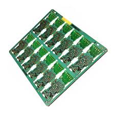
How Do Micro Vias Help in High-Density PCBs?
A final challenge is the need to prevent voids in buried microvias, which can occur during the etching process used to create the via hole. This can reduce the conductivity of the via, leading to circuit board failures such as uncontrolled current flow and shorts. As a result, the use of pulsed plating and conformal plating are critical to minimizing voids in buried microvias during the manufacturing process.
In addition, it is also important to consider the effect that the material used to construct the microvia has on its overall reliability. In particular, the choice of copper material and its plating is an important factor, as this determines how easily the plated microvia will withstand vibration, corrosion, and temperature changes over time.
While it is possible to design a PCB with microvias by using conventional drilling methods, the best way to optimize the manufacturability of your PCB is to take a DFM-centric approach when defining them in your CAD software. This starts in the layer pair and material editor, where you can build a proposed stackup and choose an appropriate laminate that will support your fabrication process. Once this is done, I recommend sending the stackup to your fabricator for review and input as to any potential manufacturability issues with the microvias you’re planning on using.
Depending on the complexity of your design, you may want to use stacked or staggered microvias. Stacked microvias run straight through multiple layers, while staggered ones are offset from one another by a few layers. This allows you to meet the density and performance requirements of your design without sacrificing reliability or manufacturability. Another option is ELIC, which stands for Every Layer Interconnection, and uses a combination of both stacked and staggered microvias.