RF PCBs used in antenna design
Radio Frequency (RF) Printed Circuit Boards (PCBs) play a crucial role in the design and development of antennas for wireless communication systems, satellite communications, radar, and other high-frequency applications. The antenna is a key component in any RF system, as it enables the transmission and reception of electromagnetic waves. RF PCBs, with their precise layout and material selection, provide the necessary platform for creating antennas that operate efficiently at specific frequencies. These specialized PCBs are engineered to handle high-frequency signals while minimizing signal loss, maintaining impedance matching, and ensuring the antenna’s optimal performance.
One of the most important ways RF PCBs are used in antenna design is by providing an ideal substrate material. Antenna performance is significantly influenced by the characteristics of the material upon which the antenna is built. RF PCBs are typically made from materials that are specially selected for their ability to handle high-frequency signals with minimal loss. Common materials include Teflon (PTFE), ceramic composites, and high-frequency laminates that offer low dielectric loss and stable electrical properties at high frequencies. These materials help ensure that the antenna performs well by allowing electromagnetic waves to propagate effectively with minimal attenuation. By selecting materials with low signal loss, RF PCBs contribute to the overall efficiency of the antenna, especially in high-frequency applications.
Another critical aspect of using rf pcb in antenna design is the impedance matching of the antenna. Impedance matching is essential to maximize the power transfer between the transmitter and the antenna, as well as to minimize signal reflections. If the impedance between the antenna and the PCB or transmission line is mismatched, the signal can be reflected back into the system, leading to power loss and degraded performance. RF PCBs are designed to maintain a consistent impedance along the signal path, ensuring a smooth transition of the signal from the PCB to the antenna and vice versa. This is typically achieved through careful routing of signal traces, maintaining controlled impedance lines, and incorporating techniques like microstrip lines or stripline configurations, which are designed to match the impedance of the antenna.
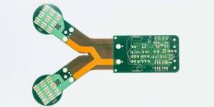
How are RF PCBs used in antenna design?
RF PCBs are also used to integrate the antenna with other circuit components on the same board. This integration is particularly useful in modern wireless devices, where space and weight constraints are critical. By integrating the antenna onto the same PCB as other RF components, such as amplifiers, mixers, or filters, designers can create compact, cost-effective solutions for wireless communication systems. This integration reduces the need for external components, leading to a more streamlined design and better performance. For example, in RFID systems or Bluetooth devices, the antenna and circuitry can be integrated on a single PCB, making the system more efficient and easier to manufacture.
Additionally, size and form factor are key considerations when using RF PCBs for antenna design. RF PCB-based antennas can be designed in a variety of shapes and sizes to meet the specific requirements of the application. For instance, antennas such as patch antennas, slot antennas, or microstrip antennas are commonly integrated into RF PCBs. These designs allow for antennas that are compact, lightweight, and capable of operating at specific frequencies. By designing antennas with the right dimensions and shapes, engineers can tailor the performance of the antenna to suit the desired frequency band and radiation pattern.
Thermal management also plays a significant role when RF PCBs are used in antenna design. RF systems, especially those operating at high power levels or frequencies, generate heat, which can impact the performance of the antenna and other components. If the temperature of the PCB or antenna rises too much, it can cause signal distortion, component failure, or reduced efficiency. RF PCBs often include features such as thermal vias or large ground planes to help dissipate heat, ensuring the antenna maintains consistent performance even under demanding conditions. Effective thermal management helps extend the lifespan of the antenna and ensures reliable operation in a range of environments.
Another significant contribution of RF PCBs in antenna design is the ability to facilitate multiple antenna configurations. In modern wireless communication systems, technologies like MIMO (Multiple Input Multiple Output) rely on multiple antennas working together to transmit and receive signals simultaneously. RF PCBs can be designed with multiple integrated antennas on the same board, enabling MIMO systems to be compact and highly efficient. These designs often involve careful planning to avoid interference between antennas while ensuring that each antenna performs optimally in the system.
Lastly, design flexibility is a major advantage when using RF PCBs in antenna design. Unlike traditional antenna manufacturing methods that may require separate components and complex assembly processes, RF PCBs offer the flexibility to prototype and test different antenna designs with ease. By modifying the layout, trace widths, and shapes of the PCB, designers can quickly iterate and optimize antenna designs to achieve the desired performance characteristics. This flexibility reduces the time and cost associated with antenna development, enabling faster prototyping and deployment of RF systems.