Limitations of High Density Interconnects
High density interconnects are an essential PCB technology that enables smaller-footprint devices while maintaining quality and performance. The use of HDI PCBs is essential in modern electronics that demand greater functionality and performance in a smaller footprint such as mobile devices, consumer gadgets, aerospace and automotive industry, and the healthcare sector.
high density interconnect PCBs are an advancement in the Printed Circuit Board (PCB) manufacturing technology that utilizes finer lines and spaces, smaller vias, and more capture pads. The technology allows designers to pack in more components into a smaller space, increasing the efficiency of the device. The PCBs can also withstand higher frequencies and more power than conventional multi-layer PCBs.
This PCB variant is ideal for challenging designs that require advanced connectivity in a compact space, including BGA with small ball pitches and multiple layers. They are used in the production of portable devices such as smartphones, PDAs and video recording devices. The technology is also employed in the production of aerospace and defense equipment such as navigation systems, radars and electronic control units.
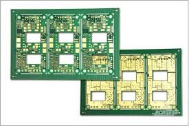
What Are the Limitations of High Density Interconnects?
Aside from the higher circuitry density, high-density PCBs are more cost-effective in the long run due to reduced design and manufacturing costs. It also enables designers to incorporate more functions into a single PCB, resulting in a lower overall weight and volume.
High-density PCBs can be more difficult to repair or rework than conventional multi-layer boards due to the tight component placement and intricate routing. Additionally, the use of blind and buried vias can cause signal integrity issues for high-speed signals requiring precise timing.
In addition, the high current densities found in HDI PCBs may lead to electromigration. This process causes metal atoms to migrate over time, creating open circuits and increased resistance. The use of proper design practices and ESD protection measures are key to mitigating these issues.
Despite these limitations, HDI technology remains strategic for packing rising functionality into shrinking footprints in today’s leading-edge electronics, including IoT products that need more compact sensing hubs and energy efficiency gains in industrial automation. It also suits the demands of emerging categories such as augmented reality, where the ability to fit densely packed sensors in a small package is critical.
To overcome these limitations, it is crucial to carefully plan the PCB layer stackup configuration prior to layout. This will ensure that the impedance-controlled routing calculations are correct while maximizing thermal and signal integrity performance. Additionally, assessing the electrical constraints early through modeling prevents common “gotchas” that could negatively impact the final product. By incorporating these optimizations, HDI PCBs can be delivered to market with confidence.